SMMMmmmm - when root is not enough
Swimming, Diving, Hopefully not Drowning!
I got a super nice project, and for that I needed to learn how the SMM really works. Again I started dipping my toes in this ocean of knowledge and I hope I don’t get too excited and drown myself before even getting started ;) For the people who are not sure if they want to read all this:
TL;DR
In SMM, it is possible to modify SMM saved execution context. SMM also sets its own IDT, it is initialized by the BIOS (DXE) and tons of cool stuff. Normally, CS base address is system-management RAM (SMRAM) base address and SMM code is copied to SMRAM in UEFI initialization and SMRAM is locked right after for security reasons.
Why use SMM? Whenever we have anything …
So important, we don’t want the kernel to screw it up
So secret, it needs to be hidden from the OS and inaccessible from direct memory access (DMA)
So sensitive, it should never be touched by anyone
… it is better to toss it into SMM ftw.
The System Management Mode
The System Management Mode, widely know as SMM, is not just yet another CPU operating mode. It is a very special small piece of technology that handles system-wide stuff. It was initially developed to handle power management ie - a resource constrained processor environment which is supposed to be transparent and isolated, used only by the system firmware (yeah, no software access intended!).
Somehow most of the BIOS researchers want to get access to SMM… Why? As researchers in the past has shown1234, attackers gaining control over SMM may potentially, in an oversimplified way, modify all physical memory, install kernel backdoors or even change the configuration of the hardware stealthily from the OS point of view. Interesting enough, in UEFI some important security features implementations use SMM, for example protecting the firmware image inside the flash.
To access the SMM environment, a hardware non-maskable interrupt is used - I am going to get into more details further down, and but the thing to remember is: this interrupt has higher priority levels than OS kernel or even hypervisors.
The System Management Interrupt (SMI)
The access to SMI is done through the SMI# pin on the processor or through an SMI message received through the APIC bus. The SMI is a non-maskable external interrupt that operates independently from the processor’s interrupt- and exception-handling mechanism and the local APIC. The SMI takes precedence over an non-maskable interrupt (NMI) and a maskable interrupt.
– Intel SDM
As you see, the SMI is generated by the chipset. To trigger it, we need to modify the Advanced Power Management Control (APMC) register.
In and Out of the SMM
As I stated in the beginning, we can enter the SMM only through SMI. When SMI is invoked, the processor will backup its context and switch to a new, separated and (hopefully!) inaccessible address space environment. The SMI handler is executed inside this environment and all OS’s interrupts are disabled. SMI can be signaled from real-addresses, protected or virtual mode.
Also interesting is that the CR4 register gets cleared - yes, all turned to zero - when entering SMM.
If a second SMI occurs while in SMM, it will be latched and executed as soon as a SMM exits occurs, usually with a RSM (resume) instruction call. Only one SMI can be latched, all other subsequent SMIs will be discarded.
The handler finishes its operations with a RSM instruction, which exists only in the SMM context. An attempt to execute the RSM instruction outside of the SMM context results in an invalid-opcode exception (#UD). The RSM instruction reloads the saved process context, switches back to the mode it was in when the SMI was called, the processor returns an SMIACK (the signal of SMI acknowledgment signal on return) on the system bus and resumes execution on the interrupted task.
The Shutdown State
If something weird in the SMRAM is detected by the processor, the dumbed shutdown state is called and a special bus cycle is generated. When the processor is in shutdown state, no instructions are executed until a RESET, INIT or NMI is asserted.
Inside the SMM - SMRAM
The SMI handler is executed inside the SMM and all critical information (code & data) lives in the SMRAM within this reserved address space created upon entry.
The SMRAM can be located in Compatible Memory Segment (CSEG), High Memory Segment (HSEG) or Top of Memory Segment (TSEG) system memory regions, depending on the hardware / platform you have. Normally BIOS developers would use CSEG. Nowadays UEFI developers mostly use HSEG and TSEG, since they offer 8MB of cacheable memory, giving them more freedom to architecture more complex drivers inside SMM. Look for the datasheet specific for your platform for the nitty-gritty details.
The interesting thing about TSEG is that no software can access it directly but it is possible to calculate where it is located:
TSEG ADDR = Top of Low Usable DRAM (TOLUD) - Size of Data of stolen memory (DSM SIZE) - size of GTT stolen memory (GSM SIZE) - size of TSEG (we can also say Thaís segment bc you know…)
There’s also other registers that should be properly configured and locked by firmware to protect SMRAM from various attacks:
- Top of Upper Usable DRAM (TOUUD), Top of Low Usable DRAM (TOLUD), REMAPLIMIT and REMAPBASE registers that used to configure physical memory map must be locked by firmware to protect SMRAM from memory remapping attacks. For more information check “System Management Mode Design and Security Issues“ and “Preventing and Detecting Xen Hypervisor Subversions“.
- TSEGMB register defines address of memory region that should be protected from DMA access, firmware must configure and lock it. For more information check “Attacking UEFI Boot Script“.
- System Management Range Registers (SMRR) — a pair of IA32_SMRR_PHYSBASE and IA32_SMRR_PHYSMASK MSRs that can be modified only by SMM, TXT and ACM code. Because HSEG and TSEG memory is cacheable — SMRR must be configured to protect it from SMM cache poisoning attacks. For more information check “Attacking SMM Memory via Intel CPU Cache Poisoning“.
– Cr4sh
The default SMRAM size is 64 KBytes and begins at the SMBASE address (0x30000 at the hardware reset, commonly seen at 0xA0000 as BIOS relocates it to the video card I/O ports). A larger area can be decoded, if needed, varying from 32KBytes to 4GBytes. The SMBASE address can also be changed. The default layout looks like this:
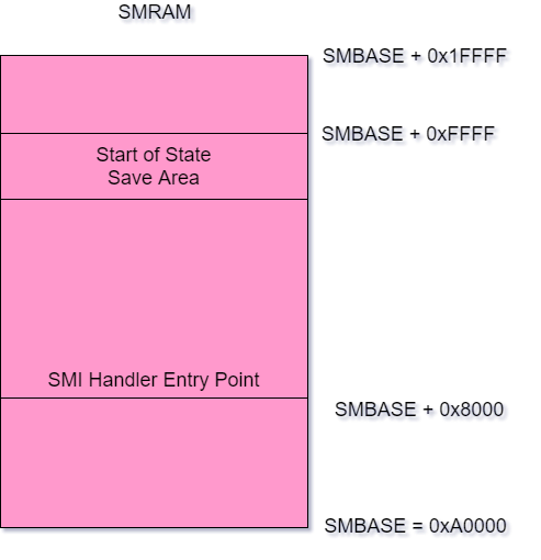 |
|---|
| SMRAM default layout - source: Intel SDM |
Standard operations which are handled by SMM would be power management of different devices / drivers, the execution of proprietary code like from OEMs and many other cool and sensitive stuff. Also all I/O and system instructions are available.
SMM code can read and modify all the saved execution context, since it lives inside SMRAM. Also SMM sets its own IDT and all, so it is the special kid in the gated community. You got the idea.
Important: Initially all the addresses are real address mode and paging is disabled (CR0.PE and CR0.PG are set to 0). The operating mode can be switched afterwards while remaining in the SMM.
Triggering a SMI
There are several ways to generate SMI:
- Ring 0 code can trigger software SMI at any time by writing some byte value to APMC I/O port 0xb2
- I/O instruction restart CPU feature allows to generate SMI on any I/O port access by IN or OUT processor instruction
- Some are accessible via PCI internal chipset registers
- You can also send IPI via APIC specifying #SMI :)
SMM Start
The SMM services are started during the platform initialization. To be more specific, when the board initializes the boot services, the DXE (Driver execution environment) dispatcher will call the SMM initial program loader. The IPL (Initial Program Load) will load the SMM services into the SMRAM and it will keep it running until a platform shutdown. SMBASE MSR can be read only in SMM and is different per CPU thread and BIOS implementation.
The SMM-transfer Monitor
The SMM-transfer monitor (STM) is a virtual machine monitor (VMM) working inside the SMM. STM is stored in a special region inside SMRAM called MSEG (Monitor Segment). A 4G 1:1 mapping page table for the STM x64 mode is generated.
Between SMM and Non-SMM Data
The main job of the BIOS is to initialize the platform and to communicate with an OS. Some BIOS provide also some services to the OS like runtime services and SMI handlers.
But there is no Intel definition on how the data transfer from non-SMM to SMM should be. This is why the UEFI Forum has defined two generic ways for the communication between OS and BIOS SMI handler. It is important to notice and remember, that OEM BIOS can also define their own protocol for communication. I am studying the UEFI BIOS, which is the state of art.
How to Communicate
The UEFI specification defines the EFI_SM_COMMUNICATION_PROTOCOL, which provides runtimes services for communicating between drivers outside of SMM and a register SMI handler inside of SMM.
Some BIOS drivers which are consuming this protocol would be BIOS DXE driver, the BIOS runtime driver and even the OS agent.
SMRAM Control (SMRAMC) register
SMRAMC controls the presence of CSEG/HSEG/TSEG regions and their accessibility from less privileged than SMM execution modes. Here’s the description of its bits:
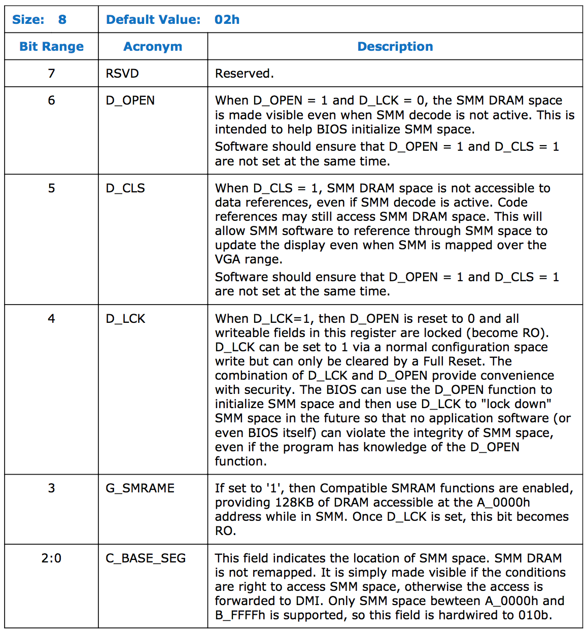
System firmware sets SMRAMC value during platform initialization and locks the register — all fields becomes read-only till the next full reset. On properly configured system D_LCK must be 1 and D_OPEN must be 0, which means that SMRAM memory will be accessible only from code that runs in SMM or higher (like an ACM). G_SMRAME field controls presence of CSEG and C_BASE_SEG is responsible for HSEG and TSEG. On my hardware C_BASE_SEG is read-only with a predefined value of 010b.
TBC
I am probably going to write more about SMM later on, keep tuned!
Good to Know:
Source:
Intel® 64 and IA-32 Architectures Software Developer Manuals
https://software.intel.com/en-us/articles/intel-sdm#combined
Building reliable SMM backdoor for UEFI based platforms (and others!!) http://blog.cr4.sh/2015/07/building-reliable-smm-backdoor-for-uefi.html
Introduction to BIOS & SMM http://opensecuritytraining.info/IntroBIOS.html
System Management Mode Design and Security Issues
http://www.ssi.gouv.fr/uploads/IMG/pdf/IT_Defense_2010_final.pdf
Preventing and Detecting Xen Hypervisor Subversions
http://www.invisiblethingslab.com/resources/bh08/part2-full.pdf
Attacking UEFI Boot Script
https://bromiumlabs.files.wordpress.com/2015/01/venamis_whitepaper.pdf
Attacking SMM Memory via Intel CPU Cache Poisoning
http://www.invisiblethingslab.com/resources/misc09/smm_cache_fun.pdf
this has been written by me for fun purposes, don't take it serious!